Science explained · Technology & Engineering
How Does a Computer Chip Use Ones and Zeros?
How can a continuous electrical voltage behave like a reliable digital bit?
Explore the sections in this article
A bit is an agreement about a physical state
A bit is an abstract binary variable with two possible values. A circuit must embody it. In common CMOS logic, voltage near the lower supply rail represents logic low and voltage near the upper rail represents logic high. Magnetic orientation, electric charge in a memory cell or the presence of a light pulse can represent bits in other systems.
The exact voltage is not the meaning. A 1.2-volt logic family might accept a range near 1.2 volts as high; an older 5-volt family uses different thresholds. Datasheets specify limits such as the maximum voltage guaranteed to count as low and the minimum guaranteed to count as high. Between them may be an undefined region.
This creates noise margin. If a gate guarantees an output high above the next gate’s minimum-high threshold, a modest disturbance does not change the interpreted bit. Logic periodically restores signals toward a rail instead of asking downstream circuits to distinguish infinitely precise analog levels.
Digital is therefore a design discipline applied to analog matter. Supply noise, temperature, transistor variation and timing still matter. A voltage lingering in the uncertain region can cause excessive current or an unpredictable interpretation.
The transistor is a controlled path
Modern logic relies heavily on the metal-oxide-semiconductor field-effect transistor, or MOSFET. A voltage on its gate terminal changes an electric field in a semiconductor channel, controlling conduction between source and drain. The simplified switch metaphor is useful: one gate voltage makes the path strongly conducting; another makes it weakly conducting. Real devices have leakage, resistance, capacitance and gradual transitions.
CMOS—complementary MOS—pairs two transistor types. In a basic inverter, a p-channel MOSFET provides a path toward the positive supply and an n-channel MOSFET provides a path toward ground. Their gates share the input; their drains meet at the output.
When the input is low, the pMOS pull-up conducts and the nMOS pull-down is off, so the output rises high. When the input is high, the nMOS pull-down conducts and the pMOS pull-up is off, so the output falls low. The truth table is only two rows:
| Input | Output |
|---|---|
| 0 | 1 |
| 1 | 0 |
During a transition both paths may partially conduct, and charging or discharging the output capacitance takes energy and time. The ideal switch picture explains logic; transistor physics explains its limits.
Gates make relationships, not thoughts
Rearrange networks of pull-up and pull-down transistors and the circuit can implement NAND, NOR and other Boolean functions. A NAND gate outputs low only when all its inputs are high. Because NAND or NOR can be composed to express any Boolean function, they are called functionally complete.
Connect gates into a half-adder and two input bits produce a sum and carry. For 1 + 1, the sum bit is 0 and carry is 1, which together form binary 10, equal to decimal 2. A full-adder also accepts a carry-in; chaining full-adders creates wider addition, though modern processors use faster carry structures.
This behavior can look like the chip “knows arithmetic.” More precisely, its circuit implements a mapping between input and output states that humans interpret as addition. Another circuit compares values, shifts bits or selects between paths. Complex computation emerges from composition, not from any transistor recognizing a number.
Binary notation scales by place value
Decimal uses powers of ten. Binary uses powers of two. The four-bit pattern 1101₂ means:
1×2³ + 1×2² + 0×2¹ + 1×2⁰ = 8 + 4 + 0 + 1 = 13.
With n bits, there are 2ⁿ possible patterns. Eight bits provide 256 patterns; 32 bits provide 4,294,967,296. The same pattern has no inherent meaning. 01000001 can be 65 as an unsigned integer, the letter A in ASCII, part of a color value or a fragment of an instruction. Circuit design and software conventions supply the interpretation.
Signed numbers, fractions and floating-point values require encodings. IEEE 754 floating-point divides a bit pattern into sign, exponent and significand fields, with special patterns for infinities and NaNs. Those conventions let different hardware and software exchange results, but rounding remains part of the representation. Many decimal fractions, including 0.1, have no finite binary fractional expansion.
A circuit needs memory to have a “before” and “after”
Combinational logic produces outputs from current inputs. A processor also needs state: registers, counters and memories that preserve information across time.
Feedback can create two stable states. In a latch, the current output helps sustain itself until control inputs request a change. A flip-flop commonly captures data around a clock edge and holds it for the next interval. Banks of flip-flops form registers near the arithmetic circuitry.
Dynamic random-access memory stores charge in tiny capacitive cells and must refresh it because charge leaks. Static RAM uses feedback circuits and retains state while powered without refresh, trading more transistors for speed. Flash memory stores charge in insulated structures that change transistor thresholds and can persist without power.
“Memory” is another functional word, not proof of recollection. A cell maintains a measurable physical state that a circuit later reads under defined rules.
The clock is a deadline, not a tiny conductor
Synchronous circuits use a clock to divide operation into intervals. Between active clock edges, signals propagate through combinational paths. Before the next capturing edge, they must settle early enough to satisfy setup time and remain stable long enough to satisfy hold time.
If a path is too slow, a register may capture the wrong value. Increasing clock frequency shortens the available interval. Designers analyze the critical path, distribute the clock with controlled skew and add pipeline stages so each stage performs less work per cycle.
A 3 GHz clock has a nominal period of about 1 / 3,000,000,000 second = 0.333 nanosecond. That does not mean every instruction finishes in one cycle or that every transistor toggles three billion times a second. Modern processors pipeline, execute multiple operations, wait on memory and adjust frequency. Different regions may use different clocks or asynchronous techniques.
If data changes too close to a sampling edge, a storage element can enter metastability, temporarily hovering between valid states. Engineers cannot abolish its probability, but synchronizer circuits and timing margins can make failure extraordinarily unlikely. The undefined middle of digital logic never disappears; design contains it.
Instructions connect hardware to software
A processor’s instruction set defines operations software can request: add, load, store, branch and many others. Machine instructions are bit patterns. Decode logic interprets fields, selects registers, chooses arithmetic operations and controls data movement.
High-level source code passes through compilers or interpreters. An expression such as total = a + b may become several machine instructions depending on language, optimization and architecture. Microarchitecture decides how a particular processor executes the instruction set—perhaps with caches, pipelines, speculative execution and multiple execution units.
No single layer is “the computer.” Meaning crosses a stack: semiconductor behavior supports gates; gates support state machines and datapaths; an architecture defines programmer-visible behavior; operating systems manage resources; applications create human-facing functions.
Why chips contain so many transistors
The first working transistor demonstrated at Bell Laboratories in 1947 replaced bulky vacuum-tube functions with a solid-state device. John Bardeen, Walter Brattain and William Shockley received the 1956 Nobel Prize in Physics for semiconductor research and the transistor effect. Integrated circuits then placed many components on one substrate, and manufacturing advances repeatedly increased density.
More transistors allow wider and more numerous computing units, larger caches, prediction structures, graphics cores and specialized accelerators. Count alone does not determine speed. Architecture, memory bandwidth, software, power and cooling matter.
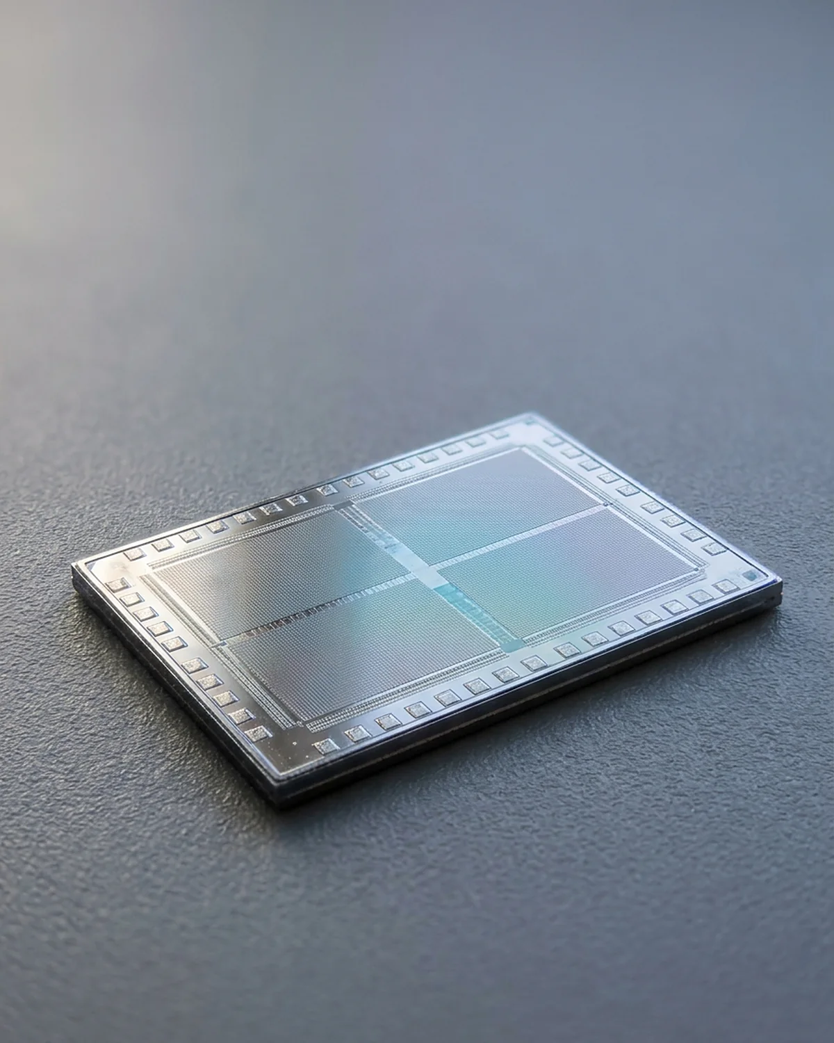
Feature-size marketing names also no longer describe one literal transistor dimension. Modern devices use three-dimensional fins or gate-all-around structures, many interconnect layers and complex patterning. A die photograph is not a simple map where each visible square is one bit.
Switching costs energy
CMOS logic draws relatively little ideal static current when not switching, but real chips leak. Dynamic switching energy is approximately related to capacitance C, supply voltage V and switching activity. A common power model is:
Pdynamic ≈ αCV²f,
where α is the fraction of nodes switching and f is frequency. The square on voltage explains why lowering supply voltage can strongly reduce dynamic power, although lower voltage can reduce speed and noise margin.
Take a purely illustrative node with C = 1 femtofarad, V = 1 volt, activity α = 0.1, and f = 1 GHz. The expression gives 0.1 × 10⁻¹⁵ × 1² × 10⁹ = 10⁻⁷ watt, or 0.1 microwatt for that effective switched capacitance. A chip contains vast numbers of nodes plus clocks, interconnect, memories, analog blocks and leakage, so this is not a processor power estimate.
Dennard and colleagues’ 1974 scaling analysis described how dimensions, voltage and other quantities could scale together in MOSFETs. That regime helped guide decades of progress, but voltage scaling later slowed. Power density became a major limit, encouraging multicore designs, specialized accelerators and aggressive power management.
Small devices face statistical physics
As transistors shrink, manufacturing variation changes threshold and current. Thin insulating barriers permit quantum tunneling. Charge consists of discrete carriers; radiation or electrical noise can disturb stored states. Interconnect resistance and capacitance delay signals. Heat changes behavior and reliability.
Fabrication therefore relies on metrology and statistical process control. Designers add error detection or correction in memories and communication paths. They test chips across voltage and temperature corners. Redundant structures can replace defective memory regions. The clean Boolean diagram is a specification implemented by probabilistic material processes.
A safe observation: build logic without touching hardware
Draw two switches in series controlling a lamp: it lights only if both switches conduct, analogous to AND. Draw them in parallel: either path lights it, analogous to OR. Then write every input combination and output.
For a genuine circuit, use a battery-powered educational logic simulator or browser truth-table tool rather than opening a computer or probing powered electronics. Change one input at a time and watch the output restore to a valid state. The exercise demonstrates composition, not transistor timing or semiconductor physics.
Does the chip really “think”?
“Think” can be a useful conversational shortcut for a whole computer system performing inference, planning or calculation. At the circuit level, it can obscure more than it reveals. Transistors respond to electric fields; gates transform logic states; memory preserves states; control circuits sequence operations. Algorithms running across those parts can exhibit capabilities that deserve serious scientific and philosophical analysis, but a logic 1 is not a thought.
The engineering achievement is already profound. Continuous voltages become robust categories. Categories become Boolean relationships. Relationships acquire state and timing. Billions of imperfect physical devices cooperate closely enough to render a photograph, forecast weather or train a model. Ones and zeros are not hidden objects inside silicon. They are the disciplined language in which we ask silicon to behave.
Manufacturing turns one logical design into variable devices
Before switching, there is fabrication. Designers describe networks of transistors and interconnect, then foundries repeat photolithography, deposition, etching, implantation and polishing across a wafer. Each layer must align with earlier layers at extraordinarily small scales. Process-control measurements track dimensions, composition and defects because a dust particle or pattern variation can disable a region.
Completed wafers are electrically tested. Dies that pass are cut, packaged and tested again across operating conditions. Yield is the fraction of fabricated dies that meet requirements. A larger die generally offers more area in which a random defect can land, so redundancy and repair are especially valuable in dense memories. Products from the same design may be sorted, or binned, by verified frequency and power characteristics rather than assumed identical.
This manufacturing reality explains why a schematic’s perfect 0 and 1 need margins. A logical design must work not with one nominal transistor but across distributions of threshold voltage, channel dimensions, temperature and aging. Timing libraries characterize cells under defined process, voltage and temperature corners; verification searches paths and states no person could inspect one by one.
Wires become a limit too
At small scales, computation is not delayed only by a transistor turning on. Metal interconnect has resistance, and neighboring conductors create capacitance. Long wires take time and energy to charge. Repeaters, hierarchy and physical placement become architectural decisions.
Memory distance is particularly costly. A register beside an arithmetic unit can deliver a value quickly; retrieving data through caches and external memory takes far longer and more energy. That gap is why chips devote enormous transistor budgets to caches and why machine-learning accelerators arrange computation around data reuse.
The binary abstraction survives all of this because each layer exposes a contract. A gate promises valid output levels and timing if its inputs, supply and environment meet specifications. A register promises stored state around an edge if setup and hold rules are respected. Architects build with those guarantees while device engineers continuously work to make them true. Digital certainty is not found in nature; it is manufactured from measured tolerances.
Frequently asked questions
Why use binary instead of ten voltage levels?
Two broad ranges are easier to distinguish reliably amid noise and device variation. Multi-level signaling and storage do exist, but they require finer sensing and trade robustness, speed, density or power.
Is a transistor literally on or off?
No. Current changes continuously with voltage, and “off” devices leak. Digital design treats selected operating regions as switch-like enough for reliable logic.
What happens between 0 and 1?
Inputs in an undefined range may be interpreted unpredictably and can make both inverter transistors conduct. During normal transitions circuits pass through this region briefly; timing and noise rules keep it from being sampled as stable data.
How many transistors store one bit?
It depends. A typical SRAM cell uses six transistors; a DRAM cell is commonly one transistor plus one capacitor; a flip-flop uses more; flash packs stored states differently, sometimes multiple bits per cell.
Does a 64-bit processor use only 64 transistors?
No. “64-bit” usually describes register and address-related architectural widths. A modern processor uses billions of transistors for logic, cache, interfaces and control.
Why does a computer get hot?
Charging and discharging capacitances, leakage current and resistive losses turn electrical energy into heat. Higher activity, voltage and frequency generally increase power, while workload and chip design shape the exact result.
Can a bit be both 0 and 1?
A classical physical node may be unresolved or metastable, but that is not a useful stable digital value. A quantum bit can occupy a superposition in quantum mechanics; measurement and error control make it fundamentally different from an ordinary CMOS bit.
Can a chip work without a clock?
Yes. Asynchronous circuits coordinate through handshakes rather than a global clock, and many chips mix clocked and asynchronous regions. Synchronous design is common because timing is easier to structure and verify.
Sources & further reading
This explainer was prepared through desk research using the sources below; established findings are distinguished from open questions in the text. See our editorial methodology.
- Nobel Prize, The Nobel Prize in Physics 1956 — Bardeen, Brattain and Shockley; semiconductor research and discovery of the transistor effect.
- Dennard et al., “Design of Ion-Implanted MOSFET’s with Very Small Physical Dimensions,” IEEE Journal of Solid-State Circuits 9(5), 1974 — historical constant-field scaling analysis.
- OpenStax, University Physics Volume 3, Semiconductor Devices — p-n junction, diode and transistor educational foundation.
- NIST, Semiconductors program — measurement science, standards and manufacturing challenges for semiconductor technology.
- IEEE, IEEE Standard for Floating-Point Arithmetic, IEEE 754-2019 — binary floating-point formats and operations.
- Chaney & Molnar, “Anomalous Behavior of Synchronizer and Arbiter Circuits,” IEEE Transactions on Computers, 1973 — metastability/synchronizer behavior in digital systems.
- MIT OpenCourseWare, “Digital Circuits: Inverter Basics,” Microelectronic Devices and Circuits — CMOS inverter operation, transfer characteristics and noise margins.
- MIT OpenCourseWare, Analysis and Design of Digital Integrated Circuits — Lecture Notes — CMOS delay and power, combinational/sequential logic, memory, metastability, interconnect and clock-distribution topic map.
Spotted an error? We correct verified mistakes promptly — email contact@flashscience.org.
Continue exploring